Author Affiliations
Abstract
1 School of Nano-Tech and Nano-Bionics, University of Science and Technology of China, Hefei 230026, China
2 Nanofabrication facility, Suzhou Institute of Nano-Tech and Nano-Bionics, Chinese Academy of Sciences, Suzhou 215123, China
3 Research Center of Laser Crystal, Shanghai Institute of Optics and Fine Mechanics, Chinese Academy of Sciences, Shanghai 201800, China
4 Hangzhou Institute of Optics and Fine Mechanics, Hangzhou 311421, China
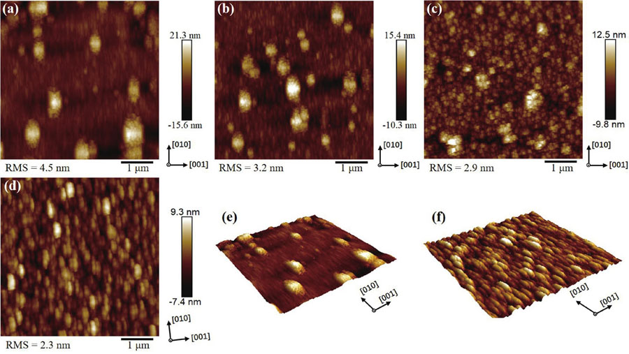
Homoepitaxial growth of Si-doped β-Ga2O3 films on semi-insulating (100) β-Ga2O3 substrates by metalorganic chemical vapor deposition (MOCVD) is studied in this work. By appropriately optimizing the growth conditions, an increasing diffusion length of Ga adatoms is realized, suppressing 3D island growth patterns prevalent in (100) β-Ga2O3 films and optimizing the surface morphology with [010] oriented stripe features. The slightly Si-doped β-Ga2O3 film shows smooth and flat surface morphology with a root-mean-square roughness of 1.3 nm. Rocking curves of the (400) diffraction peak also demonstrate the high crystal quality of the Si-doped films. According to the capacitance–voltage characteristics, the effective net doping concentrations of the films are 5.41 × 10¹⁵ – 1.74 × 1020 cm−3. Hall measurements demonstrate a high electron mobility value of 51 cm2/(V·s), corresponding to a carrier concentration of 7.19 × 1018 cm−3 and a high activation efficiency of up to 61.5%. Transmission line model (TLM) measurement shows excellent Ohmic contacts and a low specific contact resistance of 1.29 × 10⁻⁴ Ω·cm2 for the Si-doped film, which is comparable to the Si-implanted film with a concentration of 5.0 × 1019 cm−3, confirming the effective Si doing in the MOCVD epitaxy.
homoepitaxial growth MOCVD Si-doping films high activation efficiency Ohmic contacts Journal of Semiconductors
2023, 44(6): 062801

Author Affiliations
Abstract
1 Key Laboratory of Materials for High Power Laser, Shanghai Institute of Optics and Fine Mechanics, Chinese Academy of Sciences, Shanghai 201800, China
2 Center of Materials Science and Optoelectronics Engineering, University of Chinese Academy of Sciences, Beijing 100049, China
3 Hangzhou Institute of Optics and Fine Mechanics, Hangzhou 311421, China
Sb-doped crystals were grown using the optical floating zone (OFZ) method. X-ray diffraction data and X-ray rocking curves were obtained, and the results revealed that the Sb-doped single crystals were of high quality. Raman spectra revealed that Sb substituted Ga mainly in the octahedral lattice. The carrier concentration of the Sb-doped single crystals increased from to , the electronic mobility depicted a decreasing trend from to , and the electrical resistivity varied from 0.603 to 0.017 ·cm with the increasing Sb doping concentration. The un-doped and Sb-doped crystals exhibited good light transmittance in the visible region; however, the evident decrease in the infrared region was caused by increase in the carrier concentration. The Sb-doped single crystals had high transmittance in the UV region as well, and the cutoff edge appeared at 258 nm.
Sb-doped β-Ga2O3 crystal growth optical properties electrical properties Chinese Optics Letters
2023, 21(4): 041605
1 中国科学院上海光学精密机械研究所, 上海 201800
2 中国科学院大学材料与光电研究中心, 北京 100049
概述了本课题组在KDP类晶体快速生长领域的研究及进展情况。通过集成生长设备的管道系统、升级连续过滤系统、研发晶体生长过程的实时监控系统以及高精度退火设备, 实现晶体生长系统的集成化; 通过数值模拟优化晶体表面流场状态、全流程量化控制实现晶体稳定生长以及精密热退火进一步提升晶体性能; 针对点籽晶快速生长KDP类晶体中存在的柱锥交界面问题, 相继提出了长籽晶锥区限制生长法和长籽晶自由生长法, 为大尺寸高性能KDP类晶体生长提供新的技术方案。
KDP类晶体 快速生长 集成化 工艺优化 长籽晶 KDP-type crystal rapidly grown integration process optimization long-seed

Author Affiliations
Abstract
1 Key Laboratory of Materials for High Power Laser, Shanghai Institute of Optics and Fine Mechanics, Chinese Academy of Sciences, Shanghai201800, China
2 Center of Materials Science and Optoelectronics Engineering, University of Chinese Academy of Sciences, Beijing100049, China
3 School of Aerospace Engineering, Tsinghua University, Beijing100084, China
4 Department of Engineering Physics, Tsinghua University, Beijing100084, China
To reduce the seed length while maintaining the advantages of the cuboid KDP-type crystal, a long-seed KDP crystal with size $471~\text{mm}\times 480~\text{mm}\times 400~\text{mm}$ is rapidly grown. With almost the same high cutting efficiency to obtain third harmonic generation oriented samples, this long-seed KDP-type crystal can be grown with a shorter seed than that of the cuboid KDP-type crystal. The full width at half maximum of the high-resolution X-ray diffraction of the (200) crystalline face is 28.8 arc seconds, indicating that the long-seed KDP crystal has good crystalline quality. In the wavelength range of 377–1022 nm, the transmittance of the long-seed KDP crystal is higher than 90%. The fluence for the 50% probability of laser-induced damage (LID) is $18.5~\text{J}/\text{cm}^{2}$ (3 ns, 355 nm). Several test points survive when the laser fluence exceeds $30~\text{J}/\text{cm}^{2}$ (3 ns, 355 nm), indicating the good LID performance of the long-seed KDP crystal. At present, the growth of a long-seed DKDP crystal is under way.
KDP crystal long-seed rapid growth High Power Laser Science and Engineering
2020, 8(1): 010000e6


